
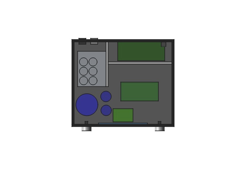
Designing the mechanical architecture for an ultra-high-end preamplifier is an exercise in compromise and spatial isolation. The design breaks down into three distinct operational domains: Analog, Digital, and Power Supply. Because the analog domain is exceptionally sensitive to external interference, the physical layout must actively prevent electromagnetic contamination from the digital engines and power rails.
Of it goes without saying, that the front and back panels have to be erogonomically layed out with intuitive connector positions, controls and the display. This is a discussion for another day. First, we have the fundementals to address.
Spatial & Electromagnetic Isolation
To protect signal integrity, physical distance and active shielding are our primary tools:
- Transformer Positioning: The high-current toroidal transformer powering the digital circuits and switching relays is placed at the absolute furthest corner from the analog boards. To mitigate low-frequency mains hum (50/60 Hz magnetic fields), the transformer will be rotated during testing to align its leakage field null directly across the sensitive circuitry.
- Digital Noise Containment: The Raspberry Pi—a high-frequency EMI offender—is mounted directly behind the front panel display assembly. Internal aluminum shielding partitions isolate the Pi’s broad-spectrum RF noise from the rest of the chassis. Screen and terminated Ethernet and USB cables will run in the digital side from the rear panel to the Raspberry Pi.
- Dual-Purpose Shielding: Aluminum partitions do double duty inside the enclosure: they block radiated RF/EMI and act as internal heatsinks for the linear power regulators.
The Core Engineering Challenges
While the primary layout is established, two critical design hurdles remain:
- DAC/ADC Module Placement: Optimizing the location of the conversion stages to minimize analog trace lengths while keeping digital bus lines (I²S/SPI) short and shielded.
- Star Grounding Topology: Establishing the exact physical node for the central star ground to prevent ground loops and shield current pollution.
Machining & Front-Panel Integration
Achieving a true high-end aesthetic requires precision CNC machining for both front and rear panels.
The front panel features a precision-milled rear pocket that allows the display to sit flush, held in place by a custom rear clamping bracket. The entire enclosure is being modeled in FreeCAD to generate the 3D STEP/DXF files required for CNC fabrication.
To keep internal wiring clean and avoid fragile DIY cable assemblies, high-speed digital IO (Ethernet and USB) uses panel-mount pass-through sockets. These allow clean, off-the-shelf shielded patch cables to bridge directly to the Raspberry Pi.
Dual Isolation & ADC/DAC Converter Placement
To achieve a vanishingly low noise floor, the ADC/DAC conversion stage is housed entirely inside the shielded analog enclosure.
Galvanic isolation ICs sit right at the boundary wall, decoupling all incoming I^2S audio clocks and I^2C control lines from the Raspberry Pi’s ground plane.
By powering the ADC/DAC clean-side using a dedicated low-dropout (LDO) regulator tapped from the main analog power supply, the converter circuitry resides entirely within the pristine Analog Ground ($GND_A$) domain.
Hybrid Grounding Topology
Instead of relying on a conventional single-point wire web, the system uses a hybrid grounding scheme:
- Digital & Analog Split: $GND_D$ and $GND_A$ are galvanically separated across the $I^2S/I^2C$ isolation barrier, preventing high-frequency Pi return currents from modulating the audio ground plane.
- Star Reference Node: The analog section utilizes a continuous ground plane that ties back to a central star node positioned between the analog PSU filtering bank and the conversion stages.
- Chassis Loop Isolation: A dedicated ground-loop breaker network (parallel power resistor, RF bypass capacitor, and safety diodes) connects the Central Star Node to the chassis ground, rejecting external ground loops while maintaining safety earth continuity.
Establishing the Central Star Point
The Central Star Point should be a heavy brass pillar or dedicated copper bus bar located inside the analog chamber, immediately between the Analog Power Supply filter capacitors and the analog inputs/outputs.
- Analog Star Connection: The GNDA plane, analog power supply ground, and ADC/DAC analog ground references meet at this single low-impedance point.ALLPCB
- Ground Loop Breaker: To tie GNDA to safety Earth (GNDCH) without creating ground loops via connected source equipment, install a Ground Loop Breaker between the Central Star Point and Chassis Ground:
- 10Ω to 35Ω power resistor (e.g., 5W)
- 100nF film capacitor (for RF decoupling) in parallel
- Back-to-back high-current diodes or bridge rectifier (for safety fault current handling)
- Isolated Side Isolation: GNDD (Raspberry Pi/digital side) must never tie directly to GNDA. Its reference terminates back at its own dedicated digital power supply filter capacitors, completely bypassing the analog star point.
Work in Progress – keeping it all shielded
With all the effort to create the screen, making the connections between the areas still remains. Here is an unfinished thoughr process that needs working out: [a chat with Gemini]
Mechanical Implementation Methods
1. The High-Speed Digital Passage (I2S & I2C)
Do not use feedthrough capacitors or steep RC low-pass filters on I2S lines—doing so rounds off bit clock edges and induces phase jitter.
- Physical Routing: Pass an IDC ribbon cable or discrete micro-coax through a precision-milled slot lined with a rubber/silicone grommet or conductive EMI gasket.
- Shield Pinning: If using ribbon cable, run an interleaving ground wire between every signal line:
[GND - BCLK - GND - LRCLK - GND - SDATA - GND]. - 360° Shield Termination: If using an outer copper braid shield around the cable, clamp the braid directly to the metal wall using a P-clip or conductive cable gland right at the pass-through point.
2. The DC Power Passage
DC lines carrying power into the analog chamber act as long receiving antennas for internal RF.
- Feedthrough Filter Capacitors: Install screw-mount or solder-mount feedthrough capacitors directly into tapped holes in the aluminum partition wall. Power enters one pin, passes through the metal wall internally, and exits the other side. High-frequency noise routes straight into the metal shield partition.
- Bulk Filtering: On the clean side immediately after the partition, place an LC network (ferrite bead in series, followed by a low-ESR 10μF capacitor to local ground).
3. Relay Control Lines
Relay lines carry step-function DC pulses and inductive kickback when switched.
- Filtered Connectors: Mount a D-Sub connector with built-in capacitive filtering (or a small transition PCB containing SMD ferrite beads and 1nF bypass capacitors) directly over a cut-out in the partition wall.
- Relay Isolation: Ensure relay coil return currents route back strictly to the digital power supply ground (GNDD), completely decoupled from the signal paths.
Recommended Layout Rules
- Avoid “Pigtails”: Never ground a cable shield via a long, thin wire soldered to the partition. Clamp the metal shield ring 360∘ against the bare, unpainted aluminum wall.
- Minimize Hole Diameter: Keep clearance holes tight around cables or grommets. An open hole acts as a waveguide; its cutoff frequency drops as size increases, letting lower-frequency EMI pass.
- Keep Isolator Chips Mounted at the Wall: Position the galvanic isolators on a PCB placed immediately adjacent to the partition wall so un-isolated digital traces do not run exposed inside the clean chamber
Suffice it to say – building all this is quite challenging!


Leave a comment