
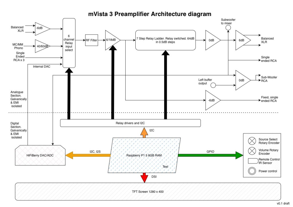
The architecture is divided into two separate sections that are physically and electrically separated. Also, great care is taken to minimise EMI and RF interference.
Analogue Section
The design philosophy is to provide the shortest path from input to output, through a minimum of devices with maximum screening.
- Dual-mono design. This means a single 4-layer PCB will cover all the analogue circuitry for a single channel. Hence, two boards create dual mono
- All input and output connectors mounted directly on the PCB to reduce added wiring complexity and keep the signal paths short and isolated
- THAT balanced convertors for XLR input and outputs
- Analogue PCB houses UL2803 relay drivers and high-quality signal relays. High-current relay power is kept well away from op amps and signal paths
- On-board ultra-low-noise LDOs (such as LT3045 modules) reduce power supply ripple to nanovolt levels.
- Designed for easy DIY assembly using entirely through-hole components (no SMD)
- Phono preamps will be separate boards
- Buffer opamps used for fixed line output and sub-woofer mono mixed outputs
- Very careful component selection. All resistors hand-matched to avoid the need for 0.1% devices. Vishay Dale CMF55 series
- High quality gold plated connectors
Digital Section
A very high-performance microcontroller, a Raspberry pi 5 with 8GB RAM, is chosen to power the Digital section, as there is considerable load to drive the hi-res screen, DAC, and streaming, all in real-time. GPU acceleration is critical to reduce CPU load.
- Intent is to mount the RPi directly on the back of the screen, ideally with the ADC/DAC HAT on-top -depends if there is enough cooling.
- Screen is the Waveshare 7.9″ 1280×400 TFT, DSI connected
- A small digital PCB to connect the off board controls eg Rotary Encoders and I2C drivers
- SW build will be based on the pyvisualiser repo
- Endpoints will deploy public repos eg Sharply, Roon bridge, MPD etc
Design Challenges & Decisions
- Whether isolation of the DAC/ADC of the digital lines and power supply is necessary. The switching speed of I2S is in the MHz, presenting potential deals and bit errors. However, EMI leakage to the analogue section is a risk. Eg using ISO7741 on I2S line
- Choice of gain and volume increments. The gain switching could be extended to 4 6dB Steps – and also whether the attenuator of 64dB is sufficient. [NB: this proved very successul with mVista 2]
- The relay attenuator targets a 1–2 kΩ network impedance—low enough to keep thermal (Johnson) noise to a minimum while remaining easy for input/buffer op-amps to drive.
- Choice of ultra-high performance ops eg bipolar at the input JFET for the buffer stage eg OPA1612 and OPA827
- Whether to use DC servo of capacitive DC blocking
- Whether to use latching relays to reduce switching noise [never noticed on mVista 2 once SW volume algorithm was correctly implemented to manage relay switch bounce]
- Whether a sub-woofer cutoff frequency control should be added on the back panel
- Cooling the Pi – this needs a fan and air circulation. With extensive GPU acceleration it runs hot
- Power supply – two separate transformer for each audio channel or is this overkill?


Leave a comment